Sound Mover - Marc MarcV8 Filter Unit
In 1995 the V8 computer controllable 8 channel filter unit was add to the Sound Moving Installation. By this not only moving of the sounds was possible but also, at the same time, dynamic timbre changes.
Back to Sound Mover block diagram
Like the SM132 unit, the V8 unit is MIDI controlled but also controllable by a parallel port. In practice both the SM132 and V8 unit are MIDI controlled to guarantee that both units are galvanic insulated from each other and the computer.
The explanation on the electronics are quite exhausting and even this does not give you all the details and aspects about the design. You are expected to know already about electronic principles more than a bit. Although the worksheets able you to copy the unit this does not mean that my explanation was intended to help you with this. I simply do some serious lalalala about it to stimulate designing electronics as an Art (versus manufacturer application imitation) |
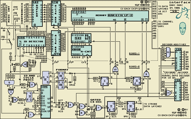
. . . Data interface Other than with the SM132 the V8 has not an individual DAC for each of its 32 parameters to be controlled. Instead it uses one 12 bit DAC that is multiplexed. This implies that the analog values that are converted from the digital value need to be stored into an analog memory. This is done by a Sample and Hold circuitry for each channel. The analog memory is build up by using a capacitor as a memory element for each analog Voltage parameter of the unit (32x). This technique has the disadvantage that the capacitors are loosing their analog Voltage due to leakage and thus they need to be refreshed continuously. To do this the interface also needs a digital memory that has each binary value stored. Otherwise it should be the computer to continuously sending data to refresh the analog memories and this not convenient because the computer needs its time to execute its choreography algorithms and to transmit data changes.
|
. . . The Job First lets see what exactly the job is that the interface must handle. Each of the 32 parameters that the filter unit counts is a 12 bit value. Thus the 8 bit memory counts 2 bytes for each parameter (divided into a 7 High bits and 5 Low bits). Besides receiving first the High bits and then - in the same data string - followed by the Low bits, the data protocol logic also need to have the intelligence to receive only the LOW or HIGH bits of the 12 bits value. This is to reduce the amount of data that need to be send by the computer (sending data by MIDI interface has a limited speed and during sending data the Atarai ST computer can not do any other task). Between each data byte which the interface receives it needs to refresh all of the 32 analog memories by fetching the data from the RAM memory, converting it into an analog value and then sending it via the demultiplexer to the sample and Hold circuitry to refresh the analog memory (this needs to be done 32 times within 32 Milliseconds).
Data protocol Principally this looks like this: 240+ID, Parameter address, Parameter value.
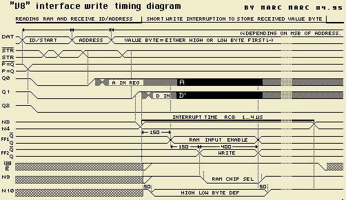
Start byte, Address byte, High byte, Low byte
The advantage is clear: flexibility in data format to optimize the software and insensitivity to data errors over a longer period (each start byte resets the logic circuitry). MIDI/Parallel switchThe double throw switch, that can be seen in the diagram. serves the function to switch from MIDI to parallel control. One side of the switch selects the STROBE input and the other side controls which incoming data lines are used. How the data format is realizedAn incoming start byte is recognized by the fact that the number is 240 or higher (up to 255). This is done by the ID DETECTOR (74HC688). It compares each incoming byte with a preset value and when they are the same it makes its P=Q output low (telling that it was the ID that came in). Also, when the value 240 is seen (thus without the ID additive) also the 4NAND gate N5 will be generate a low level. These two detected levels initialize the ID AND CYCLE PROCC. That not only the exclusive ID of the V8 unit is detected but also the value 240, which is the base value of the start byte, has to do with the fact that it must be recognized when another unit on the same MIDI line but with different ID is sending data. Because the data format allows a non static amount a bytes it must be prevented that data that is send for another unit will be seen by the V8 unit as valid. The 240 detector prevents this because it resets the CYCLE logic at each incoming 240 value. Start byteThe start byte with the correct ID however also starts via N2: the CYCLE logic (74HC194). The Strobe pulse that comes with the start byte has no effect on the CYCLE logic because it is suppressed by the fact that also a reset pulse is active at the same time. After the start byte with correct ID initialized the CYCLE logic it is ready to respond to the next byte which will be the address and its high bit definition to decide how to treat the coming value byte afterwards. Address byteWhen the address byte arrives the strobe pulse will cause the Q0 output of the HC194 to turn high. This will activate the ACTR REG (74HC574) to latch in the address to be memorized. At the same time the high bit (d7) of the address is fed to the data Flip Flop III and clocked in. This high bit appears at the Q output of FF-III and its complementary level at the NOT(Q) output. These two outputs are connected to FF-VII and FF-VIII to serve as the determining logic on how to treat the value byte(s) yet to come. Value byte When the value byte arrives the strobe pulse will set the Q1 output of the HC194 high. FF-VII will be clocked to transfer its data input (the high/low byte definition bit of the address byte which was stored by FF-III) to its Q and NOT(Q) output. When it is a high level it will go via de diode to the NOR gate N10 to set the RAM A0 address line low via NOR gate N10 which means that RAM address mode is settled for receiving the High byte of the 12 bit value.
Write pulseBy the time that these steps are settled with stable levels FF-II is clocked to generate a short write pulse at the NOT(WE) input pin of the RAM. A fraction later the NOT(CS) input of the RAM is made low via NOR gate N9. This enables the RAM and the value byte will be stored into the RAM. The time duration of the write pulse is determined by RC3. As you can see the capacitor of this network is drawn stippled - simply because this capacitor is not a individual component add to the board but the sum of the internal capacities of the NOT(reset) inputs from FF-II, I, VII and VIII. This total capacity will be large enough to generate a long enough write pulse duration with a save margin. Because the reset input of these four FF's are tied together they all will be reset after the falling edge of the write pulse. The outputs of FF-II then will follow by changing levels again. Next value byte At this point the write cycle is completed and the system goes back into the read status. A short dead time will follow (until the time duration of the pulse from N3 has passed which is determined by the RC7 network at the input of N3). Then the GATED CK OSC is started again and the refreshing actions continues. In the mean time the next data byte is on its way (busy to be converted from serial to parallel).
Some remarksYou may have noticed that the values that are send to the interface are not directly converted to an analog value to control the parameter for which it was meant to. Instead they are stored into the memory but, when the refresh action starts it will because all channels are scanned from the memory sequentially between the receiving and the write cycles. This system will only cause a maximum delay of 32 micro seconds before the binary sent value is converted to an analog Voltage to control the parameter. Although not elegant from a pure electronically aesthetic point of view it is effective and saves a lot of extra circuit design. You also may have notice that more than once certain capacitors in context to RC delay networks are drawn stippled. Like already was mentioned in context to the duration of the write pulse these capacitors are not on board components but internal capacities of the chips. The data books for the HCMOS chips determine quite exactly how large this internal capacity is and thus they can be used to function as an element of a RC network. The fact that they do not appear as board components does not mean that they are not important. On the contrary, they are of extreme importance to have the system operating correctly because they generate in combination with the serial resistors the proper delay time of several signals in the system to achieve a proper sequence of events. Write timing diagram The diagram below shows you the timing of a write cycle as a graphic which makes it more easy to understand the system.
|
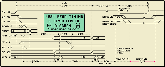
. . . Read Cycle
Requirements The timing diagram above shows you the most important digital signals for the read cycle. When not a byte is received from the computer that need to be stored into the RAM, the interface is continuously reading data from the RAM to refresh the analog memory unit. As was explained before, it was a requirement in the design to refresh all channels of the analog memory at least one time between each byte which the computer sends. When the computer sends its bytes at full MIDI baud rate the following is true: Each byte takes 1000000/31250 baud = 32 micro seconds * 10 bits = 320 micro seconds to be transferred.
A look ahead on the results To already give you the results of the realized unit; it demultiplexes at a rate of 333KHz. This implies that within 316 micro 105 times a channel can be refreshed. This high speed is quiet unusual for a demultiplexer design (synthesizer designs that often include a multiplexed system like this, mostly demultiplex at a rate of 10 to 20Khz).
Data read from RAMReading the two bytes from RAM together forming a 12 bit binary number to be send to the DAC takes 550ns (nano seconds). This is based on a 200ns Low Power RAM (6116LP-2). The circuitry to read the RAM is dimensioned in such way that all signals are within a save time area for proper operation (think about propagation delays and RC timing tolerance). Digital to Analog conversionThe conversion time of the 12 bit DAC (AM6012) including the buffer OpAmp TL072 takes 400ns plus some overshoot recovery time. All together the analog Voltage is stable after 1 micro and the demultiplexer opens the gate for the addressed channel to refresh the Voltage over the memory capacitor. Analog memoryThe 2 micro seconds time that is available to refresh the capacitor is plenty enough to restore the loss of charge over the capacitor but is not enough to fully charge it when the Voltage needs to change extremely from its lowest (zero Volts) to its highest value (5 Volts). This however is not a problem because in that case it simply will take some extra cycles to fully charge or discharge the capacitor (and you will not notice it). The advantage of high speed demultiplexingA big problem with the demultiplexer IC's like the CD4051 of HC/HCT and also with the integrated CEM5530 are the spikes that appear when channels are switched over in the chip. Secondly the stray capacities on the board also spread the switching spikes all over the place. A big mistakes that is often made by the synthesizer designers is the lack of using the Inhibit pin of the demultiplexer to reduce crossover spikes between the channels. By using the Inhibit possibility properly one can reduce this problem already quite a bit. The demultiplexer must be inhibited before the address change on the chip and made enable again after the address is internally stable. Then the channel in the chip is switched open to charge or discharge the capacitor. When the time has come that a new analog value is about to come the chip must be inhibited again.
|
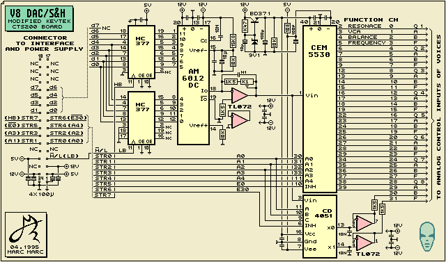
. . . DAC and S&HThe diagram below shows both the 12 bit DAC and the 32 Sample and Hold channels which store the analog voltage. DACThe two data latches (HC377) receive their data from the RAM memory from the data interface. The interface also generates a HB and LB strobe to transfer the two bytes, which appear after each other on the bus, into a 12 bit wide data register to the DAC. The DAC converts it into a current and the OpAmp converts it into a positive Voltage within the range of 0 to 5 Volts. S&H The Analog voltage from the DAC is multiplexed. On a high speed the interface reads the memory for 128 channels and send the binary values to the DAC. The Analog Voltage from the DAC then need to be demultiplexed and stored into a hold capacitor to be memorized. The CEM 5530 chip is a complete demultiplexer and S&H chip. It includes on chip hold capacitors but, it only has 30 channels. The two missing channels which are required to control the Voices are therefore build up with a CD4051 and TL072. The other channels that are read from RAM do not exist yet.
|
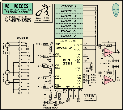
. . . VOICESThe CEM3389 chipThis chip, especially designed for synthesizers, has all the circuitry integrated for a Voltage Controlled 24dB low pass filter with Frequency and Resonance control, a Voltage Controlled Amplifier and a Voltage Controlled stereo output Balance stage. To make the chip operational as a Voice end stage only some components are required to interface the chip to the control voltages, to adjust the scaling and to set some initial parameters.
|
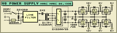
. . . Power Supply The diagram below shows the power supply for the V8 unit. It is a straight forward design with the popular 78xx and 79xx regulators. The supply delivers 3 regulated voltages for both the positive and negative supply.
|
|
For response email to This page and all contents: (C)1996 by Marc Marc Amsterdam |