|
Sound Mover - Marc MarcSound Moving InstallationThe diagram below shows you how the SM132 Sound Mover is electronically realized. When the SM132 was designed this needed to be done very quickly because projects already were running and the firm that originally was ordered to design failed in designing it with good audio specifications (they wanted to do modern and choose for a full digital design). This is why I designed with analog techniques and only with parts and principles that I knew very well without the need to verify by experimenting. Although some details I would design differently by now it was a good idea at that time. As it turned out the whole unit operated as was expected, without any mistakes (which are usually normal when designing something new). Through the years the SM132 proved to be a very reliable unit (it never has failed). The only part that I changed was the data interfacing - not because it was bad but, because the V8 filter unit was added to the system and needed to be controlled by the same computer. Therefore a data interface with an Unit-Identify mask was necessary and also it turned out to be better to control both units by MIDI rather than by the parallel port and thus a MIDI to parallel interface was add.
Back to Sound Mover block diagram
|
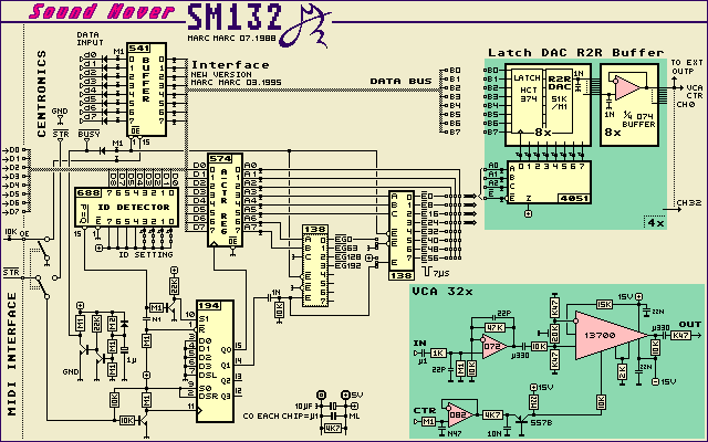
. . . Data interface At the left of the diagram you see how the parallel data is interfaced. In practice this
parallel data comes from a MIDI to Parallel interface. The incoming data is buffered by a
74HC541 and then fed to both the data bus and the control logic circuitry which handles the
data protocol to have the data be received by the right channel. The data protocol starts
with the number 240 plus the unit ID (0...15) added to it. The 74HC688 functions as the ID
detector and only will enable the other logic when it sees the correct ID set for the unit.
This ID can be set with the 4 jumpers that are connected to the ID detector. After a
corresponding ID a 74HC194 is set enable and will generate at its Q1 output a high level at
the clock input of the ACTR REGISTER of the 74HC574 when the next data byte comes in. At this
point this byte is stored into this latch and will function as the address for the channel
decoder (the two 74HC138's and a CD4051 at each 8VCA board). The next data byte (volume
value for the VCA) will generate a high level at Q2 of the 74HC194 and this will generate a
strobe pulse via the addressed channel decoder to have the data latched into one of the 32
DAC registers (74HC374).
Special attentionSpecial attention was paid when designing this interface that a hardware failure would not cause the system to hang. Even when the data protocol is not finished, it will function correct when the next data stream is coming in. This is done by having each initial data byte (240+ID) resetting the protocol logic. Also a data error from the computer will thus not cause the data interface to hang. The only thing that could happen is that due to a data error or a software mistake one or more channels get wrong volume information but, this problem is solved in the controlling software program.
Diodes in the parallel data linesYou may have noticed the diodes in the Centronics input lines. They were added to prevent that the Voltage on the parallel data lines from the computer will leak into the interface circuitry when the SM132 in off power and the computer is already on. This was relevant because the computer is turned on before the SM132 and the Voltage leak sometimes caused errors due to the fact that even the small leak current from the incoming data lines is enough for powering the interface circuitry in a bad way. The only leak current that still will come through is via the 10K pull up of the strobe input but, this effect is neutralized by putting a 4.7K resistor across the 5Volt supply of the interface. This only is relevant when the SM132 is controlled by the centronics (parallel) port of the computer. When controlled by the MIDI interface, the computer is galvanic insulated from the the SM132 (which is a must when more units are to be controlled by the same computer).
MIDI/Parallel switchThe double throw switch, that can be seen in the diagram has the function to switch from MIDI to parallel control. One side of the switch selects the STROBE input and the other side controls which incoming data line is used. |
. . . DAC R2RAt the right of the diagram you can see how the Digital to Analog Converter is build up. You may notice that each channel has its own DAC and you might think that this is quit a waste of components since I could design it also by using multiplex techniques. Your right but, as was stated before the design of the SM132 needed to be done without any time to experiment. Designing a multiplexed version without experimenting and time eating test was at that time beyond my experience. Although the cost of components are not much more than with a multiplexed version it was the soldering of the large amount of components that was a hell of a job. Nevertheless it was very successful and still quicker than designing a multiplexed version.
DAC precision In theory the linearity of a R2R DAC network is less than that of an integrated DAC IC
but, in practice - for the purpose of controlling the VCA's - this is irrelevant. When using
good components and using resistors from the same production series the result is actually
very satisfying. With a multiplexed version specific problems of feed through of the multiplex
clock signal and switching ripple of the analog demultiplexers would cause problems that need
a very careful design to be solved. My solution for the SM132 was far way less critical but,
still required a good over thought wiring (both signal and power).
|
. . . VCAAt the lower right side one of the 32 VCA's is shown. It is build up around the well known LM13700 (which has two VCA's on chip including output buffers). To achieve good specifications with the 13700 it is very important to feed it with an audio signal from a low impedance source. That's why each VCA input is first buffered by a TL072 OpAmp type input buffer. The input buffer also amplifies the input signal about 6 times to make sure that input signals of nominal level will be strong enough for a good signal to noise ratio of the VCA. The input resistor of 10K of the 13700 is dimensioned based on the input signal level and related to the two pull down resistors of K47 (which definitely must not be made of a higher value). The 13700 has the facility to set a input diode current to increase the performance of the VCA (less distortion with higher input signals and thus a better S/N ratio). With a dual 15V supply the optimum value to set the diode current at maximum rate is 13K but the value of 15K that is used here hardly leads to worse specifications.
Output amplitudeThe output of the VCA is directly connected to the on chip buffer and pulled down with a amplifying determined resistor of 2K. This 2K resistor sets the output amplification at a ratio of 1:1 relative to the input. The 10K resistor at the VCA buffer output to the negative supply is not very critical but should not be made of a high value.
Control Voltage suppressionYou also can see that a trimmer of 20K is add between the two inputs of the VCA amp with its center to ground. With this pot the feed through of the control signal of the VCA can be trimmed to a minimum (it may improve the feed through with 20dB). When trimmed the worse case feed through at some channels was measured at -60db. Actually, when the boards were build and tested at first it was necessary to replace some 13700 chips immediately because they had a naturally bad feed through specification (the untrimmed specification varies from chip to chip due to the production techniques). This worse case was measured with switching the VCA's on/off by letting the voltage continuously jump from zero to maximum voltage. In practice the control Voltage is stepped up and down. This will decrease the control Voltage feed through.
Control VoltageThe control signal first is fed to a RC low pass network to have some smoothing of the control signal. Via a buffer it is, via another RC low pass network, fed to the transistor which converts the Voltage to a Current through the 10K resistor which is connected to the 13700. The current through this 10K resistor determines the amplification of the VCA. The pull up resistor of 220K injects a little current to set the VCA at the edge of responding to a data value of 1 (0 will be off). |
. . . Power Supply The VCA's and all Operational Amplifiers in the circuities operate with a dual 15 Volts
power supply. The supply must deliver 500 mA for both sides and of high quality. I did not
use the popular 78xx regulators because it is not so hard to get much better specifications
when using the LM723 regulator IC plus power transistors.
|
|
For response email to This page and all contents: (C)1996 by Marc Marc Amsterdam |