Sound Mover - Marc Marc

MIDI to Parallel interface

The data interface that is presented here can be used for many purposes. It converts a serial input data stream to a 8 bit parallel output plus strobe pulse. The input data is Galvanicly insulated by an Opto Coupler. Electrically it is compatible with the MIDI standard (serial format 1+8+1, drive current of the Opto coupler and the Baud rate) but, you could modify the circuitry for any other specification.

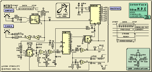
The diagram below shows you a MIDI interface that has a parallel output. Both the SM132 and V8 unit use one to have them controlled by the MIDI port of the Atari ST. When speaking about MIDI you have to realize that the MIDI protocol and the interface are two different things. The MIDI protocol is an industrial agreement (standard) between manufactures of musical instruments that describes by what numbers and how many (data bytes) certain parameters of the instruments will be controlled. The MIDI interface is an agreement on the electrical specifications of the hardware interface that sends and receives the data stream.
In case of the SM132 and V8 unit, a MIDI interface is used but not the MIDI protocol. They use my own designed protocol but, at the same time this protocol does not interfere with the standard MIDI protocol. As a result both MIDI instruments and the SM132/V8 may be controlled by the same computer via the MIDI interface.
The MIDI interface that I designed is electrically compatible with any MIDI interface . As you can see from the diagram it is not, like usually, embedded into a micro processor system. I designed it fully with standard HCMOS chips because this was in context to the SM132 and V8 unit the most practical and also more reliable (not possible to crash).

Discrete design Data input Conversion Timing Baudrate Leds


Back to Sound Mover block diagram


. . . Discrete design

It would be possible to design this interface with a micro controller but as it turned out this would not count much less parts than as it is designed now. When a micro controller should have been used there would be the need to have it programmed in assembler to be fast enough or otherwise an expensive controller should have been used. Also a good Watch Dog should have been implemented to take care about system errors. All together this did not made it very attractive to use a micro controller. That's why I researched the possibility to design it with standard HC chip's. As you can see this was a success.
The interface only counts 4 cheap HCMOS chips and one Opto coupler. It is fast, reliable and has a larger baud rate tolerance than with the standard MIDI interfaces. You could say that the design is discrete in a modern way (normally with discrete it is pointed that the design is fully done with transistors and not with integrated circuitries ).


. . . Data Input

Conform the MIDI standard the serial data at the input is fed to an Opto Coupler to insulate the receiver electrically from the sender. This has the advantage that no grounding problems between individual units occur. Another advantage is that the Opto Coupler is actually current driven rather than by a Voltage. The drive current is standardly set at a 5 mA rate. This makes it possible to use a 10 meter connection cable between the sender and the receiver.
The serial input data conform the MIDI standard starts with a start bit followed by 8 data bits and ended with a stop bit. Between sender and receiver there is no so called handshaking which means that the serial data rate (Baud rate) of both the sender and receiver need to be equal by standard agreement. For the MIDI standard this is defined at 31.250 baud.
The input data controls the LED in the Opto Coupler 6N136 (fast type) and causes conduction in the transistor of the 6N136. At the collector output the data input is present via a pull up resistor of 4K7 for further use. This data then is fed to a shift register (4094), the control logic circuitry and a MIDI THRU output stage.


. . . Data Conversion

Shift register 4094

The 4094 transfers each data bit at its input (pin 2) sequential to its outputs (pin 0..7) at the command of the rising edge of a clock pulse (pin 3). The result is that a sequence of 8 data bits will appear as parallel data at the outputs after a cycle of 8 clock pulses is completed. The control logic responds to the start and stop bit of the input data to serve the 4094 with a correct timed clock pulse sequence to convert the input data.

Control logic

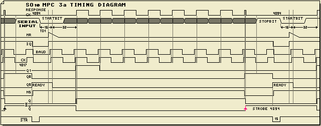
At the moment that the start bit comes in (high to low level jump of 6N136 collector output) the Flip Flop I will be set after a certain delay time (set with P40). This will cause the Q output of FF-I to jump high, the ring counter 4017 will be resetted and the baud rate generator (N1 and N2) will be enabled. The baud rate generator will generate a sequence of pulses to control the 4094 shift register. The first pulse that the baud rate generator generates after being enabled will be after half the time of its baud rate. Together with the delay time that is set with P40 at input of FF-I the first clock pulse comes exactly at the middle point of the first data bit from the input (thus the second bit of the serial data byte).
The clock pulse sequence of the baud rate generator also controls the ring counter 4017. At the outputs of the 4017 a high level will 'travel' sequentially from output 0 to 9 with each clock pulse. As you can see the 0 output of the 4017 is not used. This is because the reset of the 4017 will cause the 0 output of the 4017 to be high. When the first clock pulse comes the 1 output of the 4017 will be high and will trigger FF-II which will turn its Q output high. At this point the clock pulse can reach the 4094 clock input and thus the data bit will be transferred internally into the parallel register of the 4094. The other 7 data bits will follow at each next clock pulse.
When data bit nr 8 is transferred the ring counter 4017 will have a high level at its 8 output. This will reset FF-II via R50 and N5. The NOT-Q output of FF-II then will turn high and this will generate the STR command for the 4094 to fixated the Parallel data by transferring it from its internal register to the output latch. At the same moment the Q output of FF-II turned low and this will block any further clocking of the 4094 because D31 will keep its clock input low.
When the stop bit arrives output 9 of the 4017 will turn high. Via the RC network C3/R3 and inverter N3 a strobe pulse will be generated for the parallel output logic (to be used for further interfacing the parallel data). this strobe pulse also resets FF-I and this will cause the baud rate generator to be stopped because the Q output of FF-I will turn low and via D1 the generator is stopped (the output of N2 will turn low during this stop mode).
The illustration below shows you the exact timing diagram to visualize the explanation above.


. . . Baudrate

As was already mentioned, the baud rate needs to be the same as that of the sender. The MIDI standard is 31.250 Baud which is the same as a clock period of 32 milliseconds. With an oscilloscope or frequency counter the baud rate generator needs to be set at this proper rate by trimming with P2. When for C8 a styroflex precision capacitor is used, for R2 metal film and for P2 cermet, then a center trimmed P40 will set the baud rate already close to its proper rate.
Important is to set the correct delay time with P40 because this determines at which point the serial data in clock into the 4094 shift register For best performance this should be exactly half way the duration of a data bit. At the two version of this interface that were build the total value of P40 and R40 was measured at 18K but this also depends on the exact value of C40. When adjusted correctly the interface can handle quit a tolerance in its baud rate before errors will occur (plus and minus 6%). This will be enough to have the interface operate correctly under the full temperature range and therefore there is no need to design a baud rate generator with using a crystal (which would be more expensive).


. . . LED indication

The Led indication has two LED's: a red and a green one to create a visual check indication for the data receiving. In the diagram you find the two points that connects to the LED drivers. The red LED is connected to FF_I and will lit when data comes in. The green LED is connected to the 9 output of the 4017 and its when the data is received (constantly when no data is coming in).


For response see Marc Marc contact file

This page and all contents: (C)1996 by Marc Marc Amsterdam

Back to Sound Mover block diagram